Double sided PCB milling made easy (relatively, IMHO!!)
I wanted to make a way to repeatedly and consistently make double sided PCB. Techniques I found in internet relies on either the machine, or techniques like alignment holes, flipping
the entire stock... I don't like those techniques. I wanted something easier (for me).
This is my second year as instructor for the Fab Academy, this time in Amman, Jordan. I came here to setup the lab and decided to remain as an instructor for this cycle. One of my student
had the ISP made already and he wanted to do something beyond. He wanted to make the ISP shorter by doing it in the double sided PCB. So we decided to do that, I made my own double
sided ISP, he made his version. And for this procedure, I didn't want to show him the existing procedures as I hated them myself, instead I wanted to create a new method.
So, there it is, the background… Now let’s get back to the point.
The Secret Ingredient
The secret is in the drawing itself. Which means the whole process is
mill --> cut --> flip --> mill --> cut., simple.
I’ll explain the technique but you do the simulation in your mind :) .
Normally when you cut a board out of the stock, there will be a gap between the stock and the cut-part, the kerf, the width of the cutting tool. Now imagine, you made spacers, small
pieces, exactly the same width as the kerf, cutting tool. You can then flip the board, not the entire stock, use the spacers to align the board exactly with the previous origin.
You need to know the exact diameter of the cutting tool you are going to use, in my case it is 1/32”, but I assume 0.8mm, I like to use metric system.
First, you do the regular PCB design (I used KiCAD), draw the cutting line. I used the
Eco1.User layer for the actual PCB cutout. Then I used
Edge.Cuts layer to draw a second cutting line, which will help us do the double sided PCB easily.
As you see in the above picture, the yellow lines are
Edge.Cuts layer and the green ones are
Eco1.User layer. The the yellow lines will be used to cut the board out after milling the top layer, then we flip the board, mill the second layer and then use the green lines to cut the
actual board shape. The lines are exactly 0.8mm thick, and this will allow the bit to go exactly on the line and cut out the part within.
The outer cut lines
This is the important part. You must have noticed that the shape is not exactly a rectangle, the extra part projecting outward in the top right and the bottom left is offset by exactly
0.8mm, the same width as the cutting bit used. These projections will make sure that the board is aligned perfectly when you flip them.
The projections should not be longer than half of the length of the corresponding sides, otherwise you won’t be able to flip the board, the projections will block it from happening.
Also, note that the yellow and green lines are merging together at some locations, but this is not necessary, I did it to save material,
but Yellow should never cross the green and go inside.
Making the PNGs for the fab modules
This step is only for Fab-Modules, if your machining process uses something like Gerber, this not for you, but general idea remains the same.
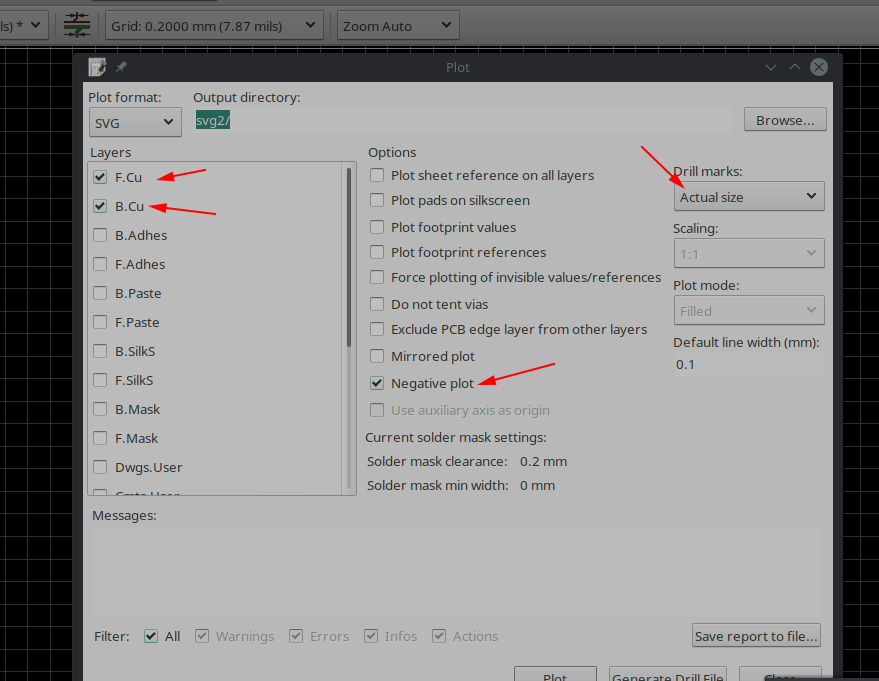
I used plotting in SVG to get the milling and cutting files. The layers were,
F.Cu, B,Cu, Edge.Cut and Eco1.User
Make sure that you select 'Negative Plot' and 'Actual Diameter' settings, as shown in the picture below.
I have created short videos showing the entire procedure from KiCAD to the final pngs.
Drawing the cut lines in KiCAD and exporting in SVG.
The plotting will give you files as seen below.
front copper layer
back copper layer
inner cut line
outer cut line
It's important that the first three files also have the outer cut line, this is how you can ensure that you can crop them all to the same exact size and aligned.
Now we will use Inkscape to extract the pngs.
Extracting the png from svg plots.
Now you will have 3 files as seen below.
front copper layer
back copper layer
inner/final cut line
Final step, making the actual cutting/milling files for Fab-Modules
There is a small mistake in the above video, but the general workflow is the same. The step generating the first cut file is wrong. You should make the line black and everything else white, this will preserve the T-bone, structure.
You will now have all the milling, cutting and drilling files ready.
front copper milling file
via drill file
first cut/outer cut file (you will flip your board horizontally after this)
back copper milling file
inner/final cut file
Milling
After processing, you will get 5 files like seen above (or four, if you have only one file for cutting and drilling vias).
This is the after the milling of the top surface, and drilling the vias.
This is after the flipping, we flipped it horizontally, you can also do it vertically, you will then have to flip the design files accordingly.
Notice the notches in the top left and bottom right corners, I had to manually cut them, so that the board goes in. I forgot about this when I did it the first time. Later I've
added them to the design, as T-bone structure. You can use T-bone or Dog-bone structure or manually cut the notches as I did. After milling the bottom layer, look how well the vias are aligned.
This is after the final cut, we now have our board.
This is my board after cleanup and tinning, just before populating with components.
what Next
My friend Yadu suggested that you can take normal png files of a double sided board and add this special cut line to it. Which is true, you can generate this cut line with some tool
like OpenScad and add them to the file.
A better way would be to use a script that takes the tool diameter and the png files as input and generate the output file with the correct cut-lines.
The ultimate way to do this would be, if possible, a script that takes the vector file, like the svg plot or Gerber, automatically do all the processing to generate the final png
images.
I think I'll be working on the last option. First option is easy and for me, there is no advantage as I'm doing the design and processing anyway, so I may as well do the extra lines
in KiCAD.

 front copper layer
 back copper layer
 inner cut line
 outer cut line
 front copper layer
 back copper layer
 inner/final cut line
 front copper milling file
 via drill file
 first cut/outer cut file (you will flip your board horizontally after this)
 back copper milling file
 inner/final cut file


